Author ELECTRONOOBS
06/05/2019
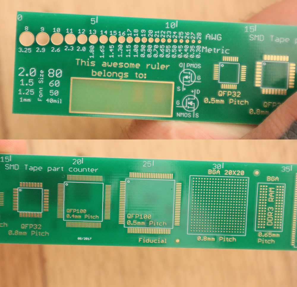
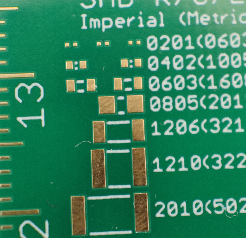
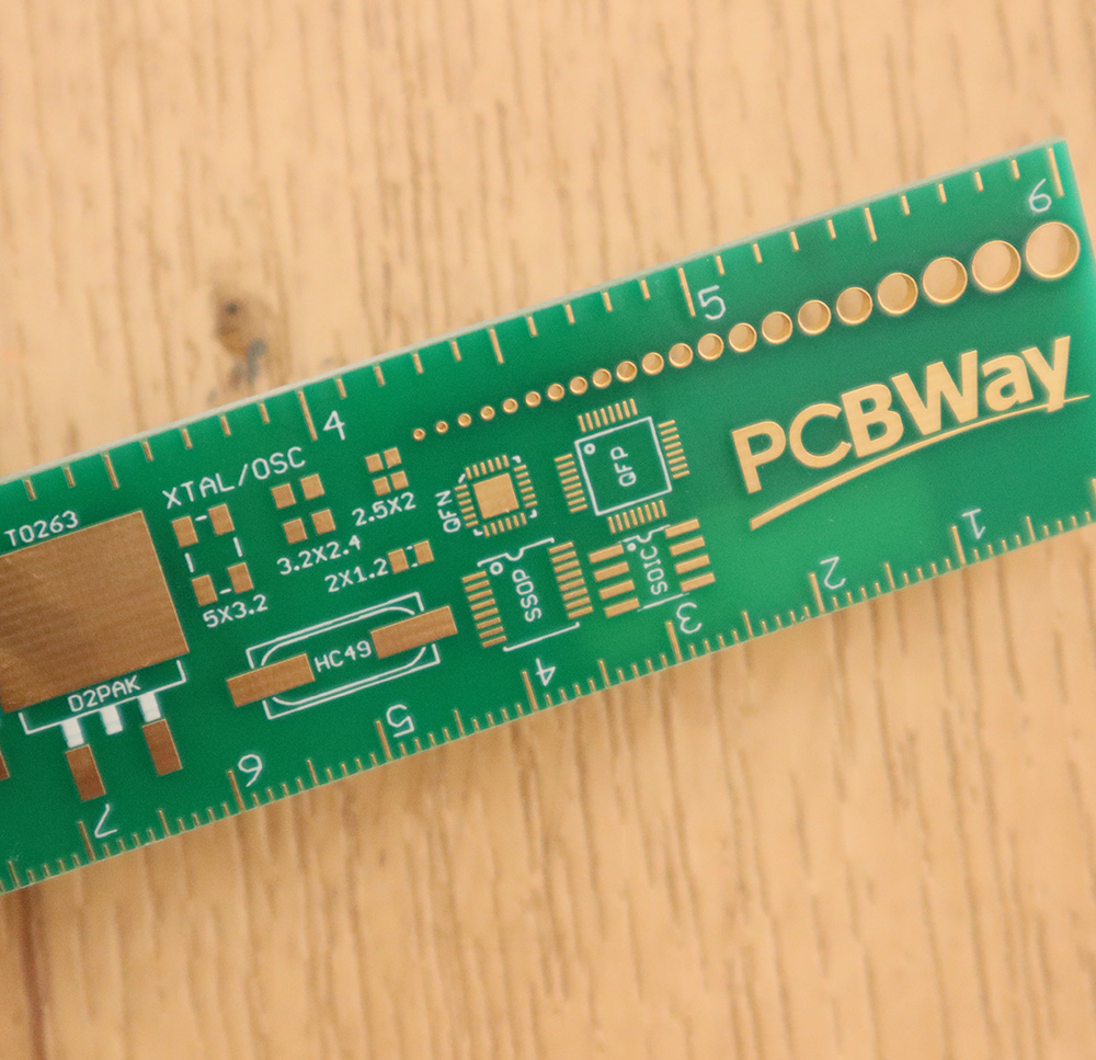
Today I've received a few PCB samples from PCBway to share with you guys. I'll go with one at a time and we start today with this PCB rule that has some sort of test prints on it. We can see the hole/via size and quality, we can see the smallest pads we could get, we can also see the gold dinish and the precision of the soldermask over the pads. So, I've received this PCB and after a first quick inspection, I can confirm that it has no errors. In this picture we can see a few types of component packages. But first, we can see the holes examples from 3.25mm to very small via of 0.3mm and these are all gold plated. They can go even smaller down to 0.2mm. In the same photo we can see a zone without soldermask or copper and the fiberglass PCB can be seen.
If you want to order your own PCBs, use
PCBWay.com and select your color.


