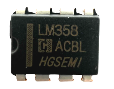
The LM358 is a dual op-amp IC integrated with two op-amps powered by a common power supply. It can be considered as one-half of the IC 74LS138 quad op-amp, which contains four op-amps with a common power supply. The LM358 series consists of two independent, high-gain, internally frequency-compensated operational amplifiers designed specifically to operate from a single power supply over a wide range of voltages. This article provides an in-depth comparison of the LM358 and 74LS138, focusing on their functionalities, applications, and key specifications.
Utilizing the circuit designs perfected for Quad Operational Amplifiers, these dual operational amplifiers feature low power drain, a common-mode input voltage range extending to ground/VEE, and single supply or split supply operation. The LM358 series is equivalent to one-half of an LM324. These amplifiers have several distinct advantages over standard operational amplifier types in single supply applications. They can operate at supply voltages as low as 3.0 V or as high as 32 V, with quiescent currents about one-fifth of those associated with the MC1741 (on a per amplifier basis). The common-mode input range includes the negative supply, eliminating the necessity for external biasing components in many applications. The output voltage range also includes the negative power supply voltage.
This article provides a basic overview of the LM358 Dual Op-Amp, including its pin descriptions, features, and specifications, to help you quickly understand what LM358 is.
- Short Circuit Protected Outputs
- True Differential Input Stage
- Single Supply Operation: 3.0 V to 32 V
- Low Input Bias Currents
- Internally Compensated
- Common Mode Range Extends to Negative Supply
- Single and Split Supply Operation
- ESD Clamps on the Inputs Increase Ruggedness of the Device without Affecting Operation
- Pb-Free Package May be Available. The G-Suffix Denotes a Pb-Free Lead Finish
- Transducer Amplifiers
- Conventional Op-Amp Circuits
- Integrator, Differentiator, Summer, Adder, Voltage Follower, etc.
- DC Gain Blocks, Digital Multimeters, Oscilloscopes
- Comparators (Loop Control & Regulation)
- Active Filters
- General Signal Conditioning and Amplification
- 4- to 20-mA Current Loop Transmitters
The IC 74LS138 is a 3-to-8 line decoder integrated circuit from the 74xx family of transistor-transistor logic gates. Its primary function is to decode or demultiplex applications. The configuration includes a 3-input to 8-output setup. This IC is mainly used in high-performance memory decoding or data routing applications, helping to minimize system decoding effects in high-performance memory systems. It features three enable pins (two active low and one active high), reducing the need for external gates. A 24-line decoder can be implemented without external inverters, while a 32-line decoder requires a single inverter.
This IC is mainly used in demultiplexing applications by using an enable pin as a data input pin. Additionally, the inputs are clamped with Schottky diodes, which provide high performance, help contain line ringing, and simplify system design.
The features of the 74LS138 IC include:
- Designed for high-speed operation
- Decoding capability
- Integrates 3-enable pins to simplify cascading
- ESD protection
- Uniform propagation delays
- Supply voltage ranges from 1.0V to 5.5V
- Inputs allow voltages higher than VCC
- Standard propagation delay is 21ns
- Low power consumption: 32mW
- Schottky clamped for high performance
- Operating temperature range: -40ºC to +125ºC
The applications of the 74LS138 IC include:
- Line decoders
- Memory circuits
- Servers
- Digital systems
- Line demultiplexing
- Telecom circuits
The LM358 and 74LS138 ICs serve fundamentally different functions. The LM358 is an analog component used primarily for amplification and signal conditioning, while the 74LS138 is a digital component used for decoding and data routing. This fundamental difference defines their roles in electronic circuits.
Both ICs are designed with power efficiency in mind, but their power consumption characteristics differ due to their different functionalities. The LM358, being an analog op-amp, has low power consumption suitable for battery-powered devices. The 74LS138, although a TTL device, is also designed to consume minimal power, which is crucial in large digital systems with numerous ICs.
The LM358 operates over a wider voltage range (3V to 32V for single supply) compared to the 74LS138, which typically operates within the TTL voltage range of 4.75V to 5.25V. This makes the LM358 more versatile in terms of power supply requirements.
The applications of these ICs rarely overlap. The LM358 is essential in analog applications such as sensor interfacing, signal amplification, and active filtering. In contrast, the 74LS138 is integral in digital systems, particularly in address decoding, data routing, and control circuit implementations.
In summary, the LM358 and 74LS138 ICs are critical components in their respective domains—analog and digital electronics. The LM358 excels in low-power, analog signal processing applications, while the 74LS138 is indispensable in digital circuit design for decoding and data routing. Understanding the distinct functionalities, specifications, and applications of these ICs is crucial for designing efficient and effective electronic systems.