When it comes to things that hackers build, PCBs are a sizeable portion of our creative output. It’s no wonder – PCB design is a powerful way to participate in the hardware world, making your ideas all that more tangible with help of a friendly PCB fab. It’s often even more lovely when the PCB has been designed for you, and all you have to do is press “send” – bonus points if you can make a few changes for your own liking!
A lot of the time, our projects are untrodden ground, however, and a new design needs to be born. We pick out connectors, work through mechanical dimensions, figure out a schematic and check it with others, get the layout done, and look at it a few more times before sending it out for production. For a basic PCB, that is enough – but of course, it’s no fun to stop at ‘basic’, when there’s so many things you can do at hardly any cost.
Let’s step back a bit – you’ve just designed a board, and it’s great! It has all the chips and the connectors you could need, and theoretically, it’s even supposed to work first try. Now, let’s be fair, there’s an undeniable tendency – the more PCBs you design, the better each next one turns out, and you learn to spend less time on each board too. As someone with over two hundred PCBs under her belt, I’d like to show you a bunch of shortcuts that make your PCB more helpful, to yourself and others.
There’s a few ways that you can share your PCB projects in a more powerful way – I’d like to point out a few low-hanging fruits, whether README.md files or markings on the PCB itself. I’ve been experimenting quite a bit with external and embedded documentation of PCBs, as well as PCB sharing methods, got some fun results, and I’d like to share my toolkit through a few punchy examples and simple tricks. I’d also like to hear about yours – let’s chat!
Most of us start with a PCB covered with reference designators, and that’s fine – it’s the default for many PCB tools, after all. Make sure you’re not forgetting a few important things, though! After all, blank PCBs are indeed mysterious, but it’s a bit of an artform to pull off a blank PCB and not have it be a pain afterwards.
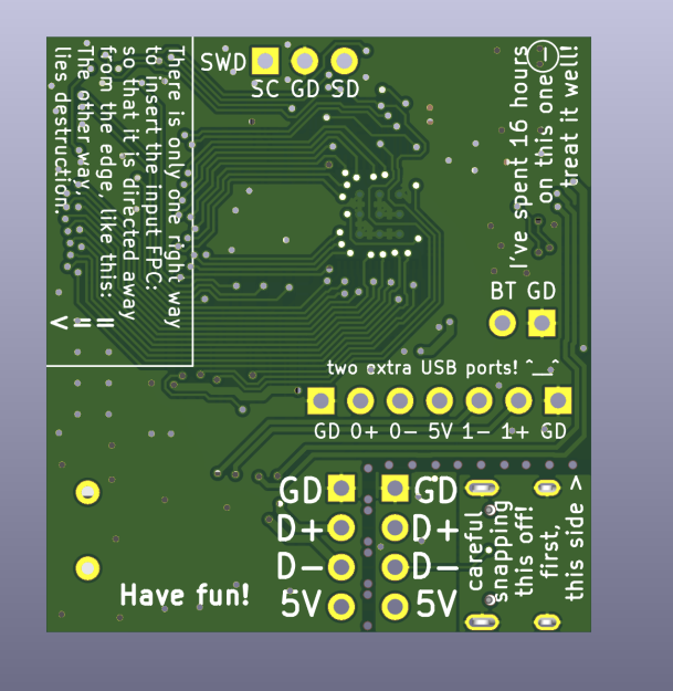
For a start, there’s a lot of place on your PCB, for things you might not have thought of. You will forget some things, you will mix some things up, and any other person who you give it to, will know even less – if you use silkscreen in certain ways, you can make your PCB not just connect things together electrically, but also keep you informed about its purpose, capabilities and limitations.Is there a warning that users of your PCB should keep in mind, even if the only user would be you, but in the future? Put it on the silkscreen! For instance, input voltages and polarity for power connectors – if it’s not using some standard connector, be it USB or PS/2, at least putting small ‘+’ and ‘-‘ on the PCB is wonderful, and doubly so if you have a battery holder!
Even if your input is USB-A or MicroUSB, which is a great proxy for “5V input”, it might be worthwhile to mark your amperage if your board would use more than 500mA-1A – since, often, USB ports can only provide that much.
Pinouts are useful to have as a reference, but they’re a kind of warning, too – an extra check before you plug something in. They also save a ton of time when you’re wiring things up – having to distract yourself and check a datasheet, a PCB image or even a KiCad window while soldering can sure slow you down.
As a guideline, every connector deserves its pinout marked on the silkscreen, on all sides it could be approached from. Let’s be fair, if desktop motherboards would put pinouts for the front panel headers on the silkscreen instead of burying them in the manual, we’d all be just a tiny bit happier. In those moments when you have the PCB on your hands and you’re eager to put it to use, it’s a bit frustrating to have to refer to the user manual for pinouts – and so often, there’s a way to fit them on the silkscreen, putting in a bit of care for the future you, or anyone else you’ve entrusted with a PCB of yours.
Of course, you might not always have space. That said, you can still do abbreviations – the QWIIC-like “GND VCC SDA SCL” can be shortened to “G V D C” if you must. You can also do things like changing pad shapes to delineate different power pin types – for instance, always use the square pad for GND. Oh, and the silkscreen isn’t the exclusive place for your text – you can put on text on the soldermask layer for either silver (HASL) or golden (ENIG) lettering, or perhaps, do higher-resolution text on the copper layer if you have enough PCB space. You can even put markings on the copper inside your pads, remember?
Do you need to add all of these? No! Do you want to add at least some of these? Absolutely! Pick the things you feel like are easy for you, make them into habits, and you’ll quickly gain skills in making your boards speak for themselves.

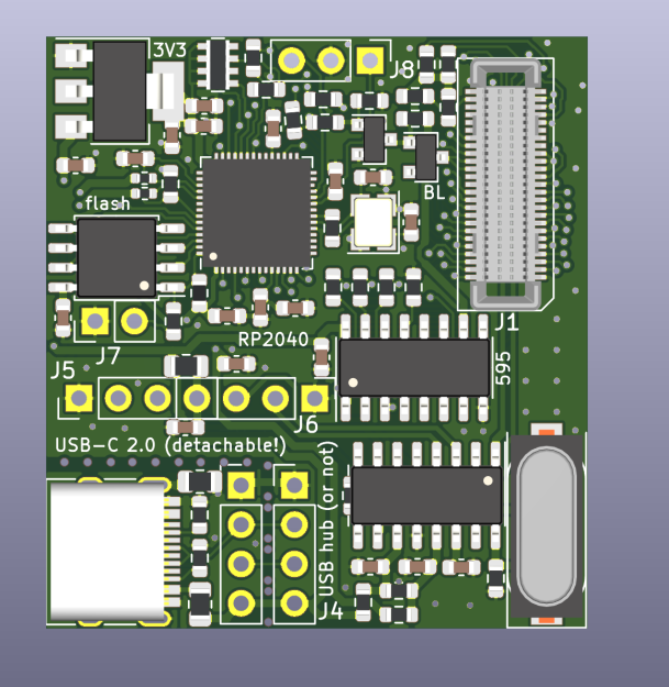
Here, I’d like to argue against putting reference designators on your PCB silkscreen- you know, things like R3 or C149. Unless you have heaps of space on a board, consider this – there’s lots of other things that take priority, and the more packed your board is, the smaller is the amount of place you have for these things. Reference designators contain a ton of information, they’re visual clutter, arranging them takes a good chunk of time, and they’re exceptionally situational. From my experience, pinouts, instructions, warnings and descriptions are worth their weight in gold, and reference designators just, aren’t. Sure, the user might be interested in knowing that the barrel jack is marked J1 on the schematic, but do they know what voltage range is it intended for? Which one would you like them to keep in mind? Which one of these would you want to quickly check as you experiment?
Erasing all reference designators is super straightforward. Afterwards, you’re left with a ton of extra space – somewhere you can put your pinouts, instructions, diagrams, or even hopes and dreams. I personally don’t put reference designators on boards, and if you haven’t yet considered removing them, I recommend that you do.
You might argue there are good reasons for reference designators sometimes, and to that, I agree – it’s just that they’re situational. Your board house shouldn’t need designators – a large amount of PCBs are nowadays released without them, anyway, and you can always provide them with a PCB picture that has the F.Fab and B.Fab layers exported instead. Thinking about releasing rework instructions for your userbase? You should provide pictures either way.
I usually leave reference designators for things like jumpers, crucial parts like user-adjustable current setting resistors, and connectors – beyond that, it makes little to no sense to have references taking up space on the silkscreen.
Now, there’s something that’s often missing from published PCBs – and that is a README file. It’s a bit painful to open a Github link and see nothing but a <code>kicad_pcb</code> and <code>kicad_sch</code> file – these are sufficient, but I’d like to know more about what your board does, beyond the filename. and it’s not hard to add either!
et’s say you’ve just designed a PCB. You’ve just put a metaphorical point in your project, and you have the entire context in your mind still, and it’s a satisfying point to be at – ain’t that wonderful! While you have ever aspect of the board available on a moment’s notice, open a README file in your text editor and spend a minute-two dumping your brain’s contents into a text file. What does your PCB help with? Which chips or parts are crucial for its purpose? Isn’t it wonderful that the PCB is done, and don’t you want the world to know about all the cool features you added?
So, write it all out, as much as you feel like it, but write something. You only really need a sentence or two for a sufficient README, and if you’re not too tired, you might find yourself writing a few more. However many sentences you write, it matters that a README is there. I personally start with a template that lists a few commonplace board things and pre-filled metadata fields, and also has things like disclaimers about the design being untested or unfinished – quite worthwhile to have!
There’s more uses for a README – for instance, whenever you’re releasing a new version, you can add a section describing what changed, what got fixed, what got added or removed – just put them as bullet points in the same README. This helps in debugging, and also informs the user that there’s more than one version of this board in existence.
Some of my personal projects are on their fifth revision, with the PCB’s looks having long stabilized. Having the version number on a visible spot has been a lifesaver of a practice – especially when I’m dealing with a PCB where v2 just works, but v1 requires an intense magnet wire fix. Unlike with software, the PCB version can be a single number – the PCB release cycle is way slower than software, so things like semver would just be wasted PCB space.
With my PCBs used by me a lot, and sometimes even used by other people, I’ve come to a short naming formula that works well. On the silkscreen, I put “BOARDNAME by AUTHOR, vVERSION” – for instance, “PS/2 to USB adapter by Arya, v1”. It’s short and sweet, and even if you don’t have any energy to work on the board’s silkscreen, perhaps this is the thing that can stay.
With PCBs, sometimes you want to share them with everyone else, but even if you don’t intend to, you still have to share them with you from the future. These few aspects matter, and as you learn to prepare , you’ll find that your work is more useful to others than ever.