
Well, surface-mount technology (SMT) is a method in which the electrical components are mounted directly onto the surface of a printed circuit board (PCB). An electrical component mounted in this manner is referred to as a surface-mount device (SMD). Imagine you already have your design of the PCB and all the components. You order a prototype of the PCB and solder all the parts. You give it a test and it works perfectly. Well, now you want to sell it as a product. But making them manually at home might take too much time. That's why you need a SMD service. You send the files to the manufacturer and receive the boards already assembled and even tested. Cool, right?
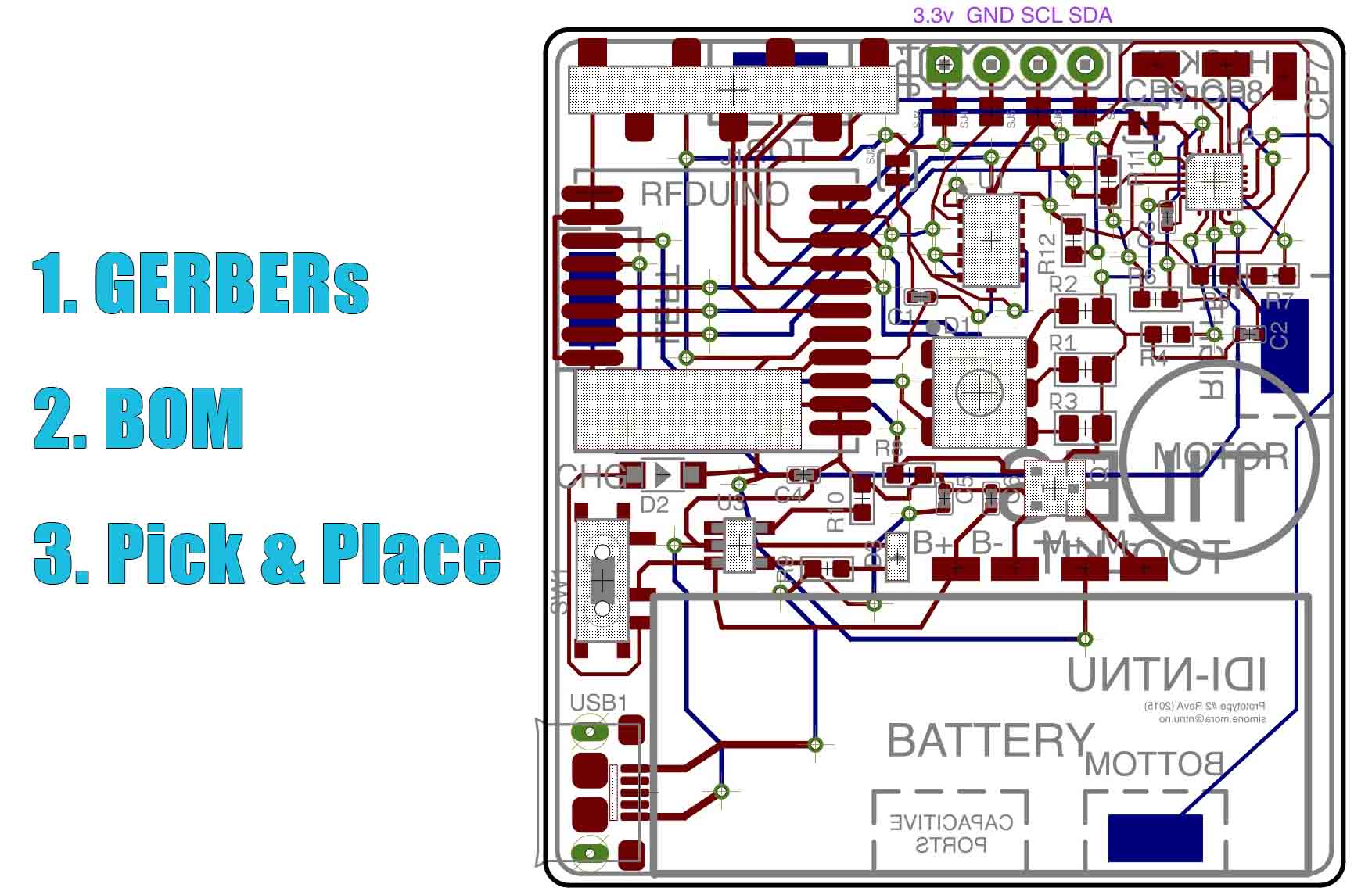
First thing is to make a design of the PCB. You can use any designing platform that you want, I usually use EasyEDA because is very easy to use and then get the needed files. Once you have the design, is recomended to order a prototype first from JLCPCB for example and test it manually in order to make sure that it works. Once you know it works for sure, you can use that design and order the SMT service. For that you will need 3 different files, the GERBERs, the pick and place and the BOM file. You can donwload those directly from your PCB editing software.
But one thing to have in mind while designing. You must make sure that the manufacturer will have the components that you are using in stock or easy to get. Otherwise, you might send them the files for SMT assembly but they might not find the components you have used. But don't worry, JLCPCB has over 230.000 of different components in stock and they are getting more and more each day. You can check all the components HERE and once your find the one you want, add it to your design and like that you make sure it will be in stock. At least that's how I do it.
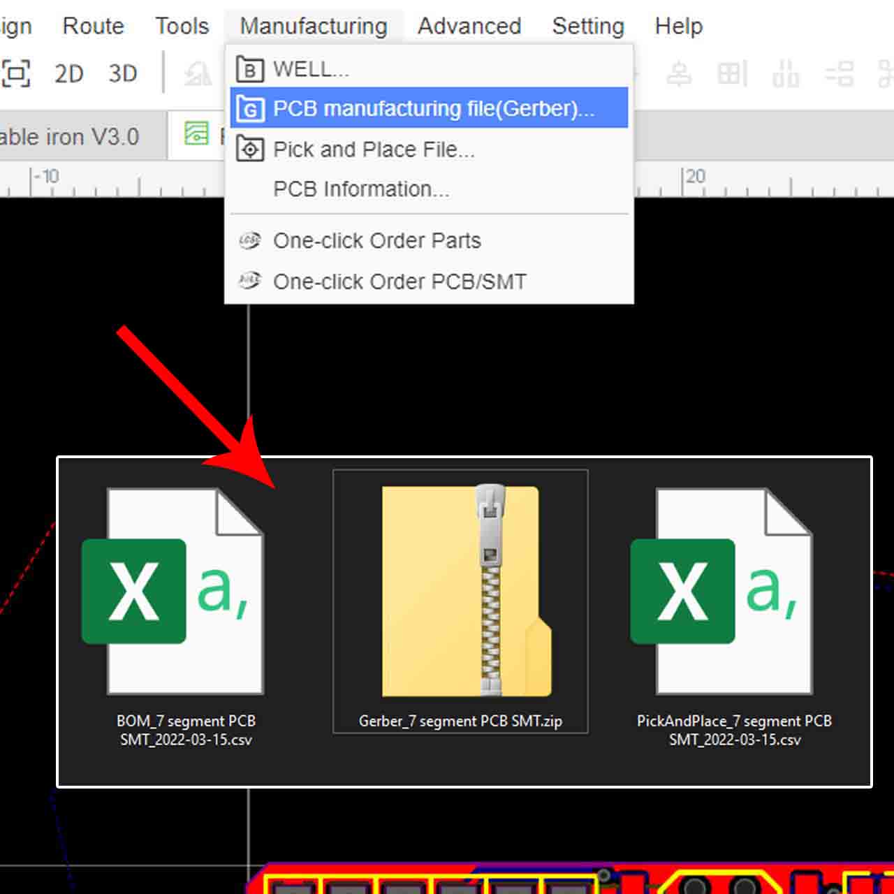
Ok, so you now have your design. Go to your download button and downlaod the GERBER files first. In EasyEDA , in PCB layout mode, you must go on the top menu and click manufacturing > PCB manufacturing file (Gerber) and download them. You will see that all the files are downloaded inside a .ZIP file. Then go again to manufacture and also download the Pick and Place and BOM files. These two are downloaded in an Excel sheet format. Have these 3 files prepared for the next step.
They have a new SMT global surcing parts service where you can find more than 230.000 parts ready to use with your projects. You can check more information about this service here. These parts are already in their stock so assembly will be very fast and secure. You don't have to care about finding the components with external suppliers.
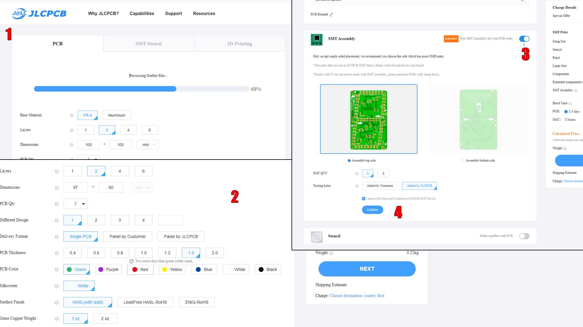
Go to JLCPCB.com and click the PCB Assembly button for quote now or go directly to this link. First you have to upload the GERBER files you have downloaded on the previous step. (1) Click the Add gerber file button and from your PC select the .zip file with the GERBERs. (2) Then you have to add the PCB settings for layers, thickness that you want, color of the soldermask and so on. Below the PCB settings you will find a toggle button for SMT Assembly. (3) Toggle it and that will activate the SMT Assembly and you will see that JLCPCB will ask you on which side you have the SMD components. Thats because for now they only solder the components on one side, they won't solder on both sides. For example select "Assemble on top side". (4) Then click the confirm button.
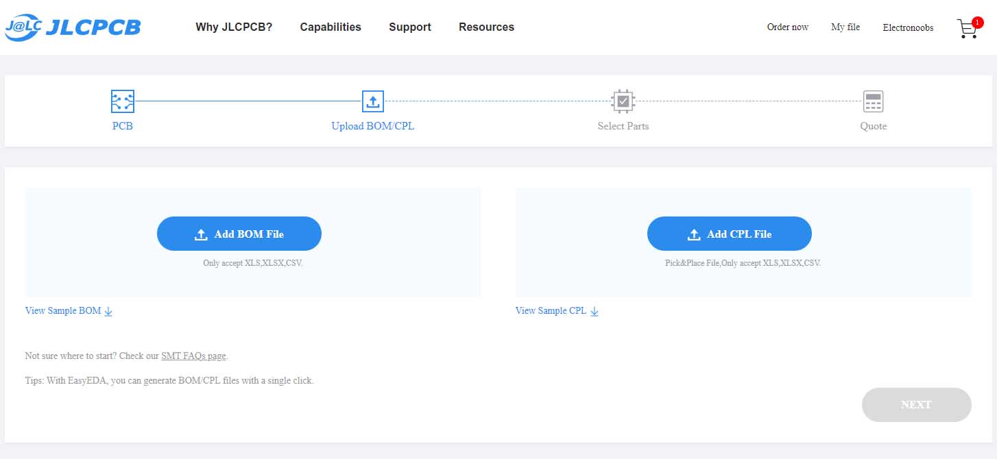
Once you've uplaoded the GERBERs and selected the settings and also enabeled SMT assemble, we click next. On the next page you have 2 buttons. Click the first one and from your PC select the downloaded Excel file for the BOM. A BOM file will have the list of all the components with their values, manufacturers and maybe an ID number. Then click the second button and upload the Excel file for the pick and place. This file has all the coordinates for each component so the autoamtic machine would know precisely where to place each one. Then click next
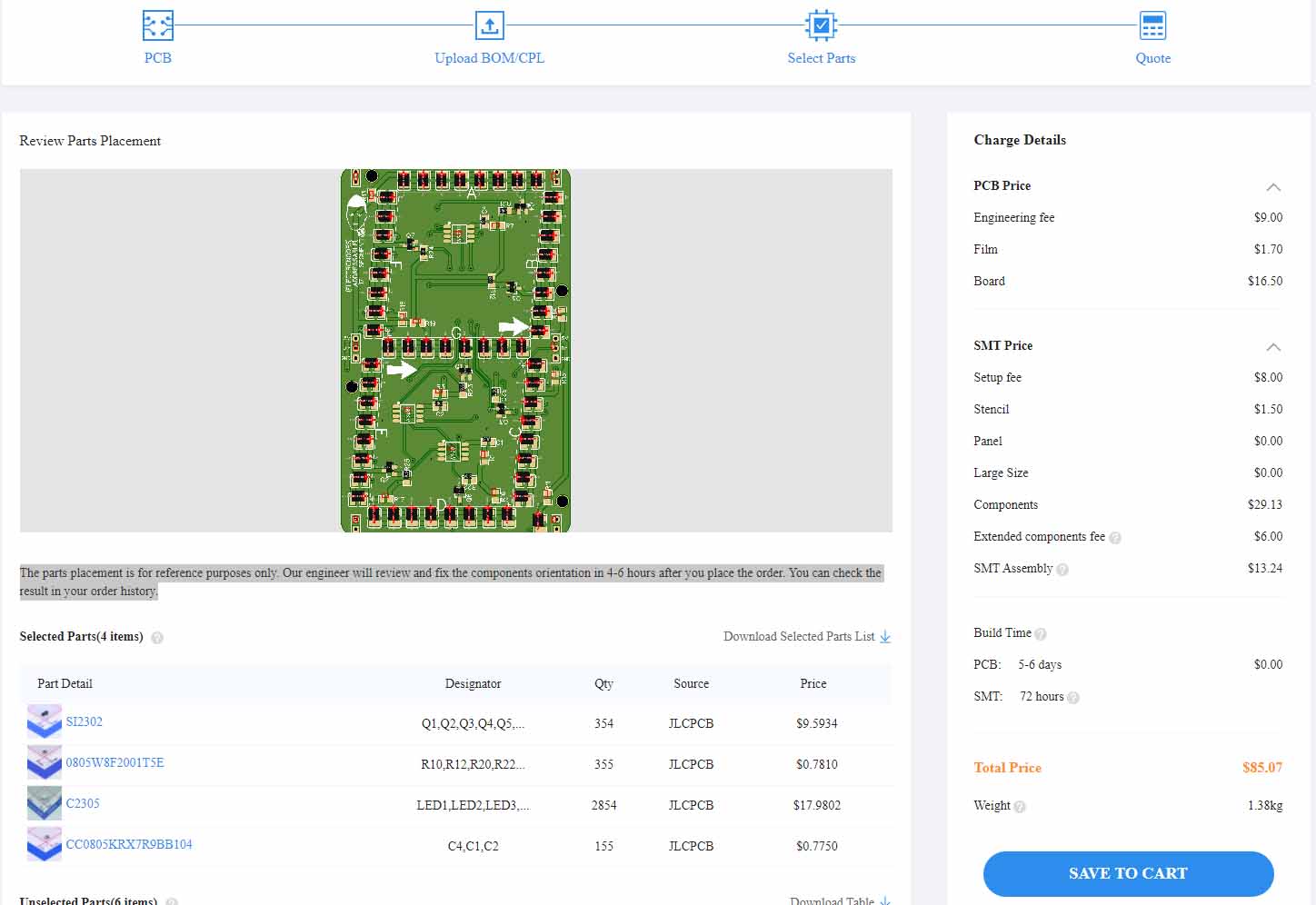
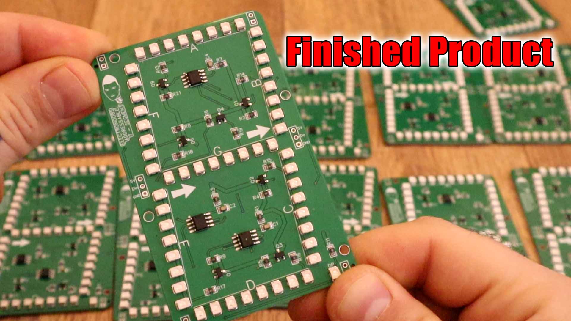
Once you've uploaded all 3 files, click next and on that next page you can first confirm the components. JLCPCB will give you a list with your selected components and also the stock they have for each component. If any of the components stock is low, you have the option to search for a new component and repalce the one that has low stock. Confirm each component and click next. On the next page we can se a real time view of the final PCB with the components in their palce. Note* that the parts placement is for reference purposes only. JLCPCB engineers will review and fix the components orientation in 4-6 hours after you place the order. You can check the result in your order history. At this point if any components appears backwards on the real time view, don't worry, they will check the correct orientation. Click save to cart and wait for the check and confirmation. Make the payment and you will receaive the PCBs assembled and ready for use.
On JLCPCB one-stop online platform, customers enjoy low-cost&high-quality&fast SMT service at $8.00 setup fee($0.0017 per joint). At the same time they assemble electronic products from PCB design to PCBA products on the same online platform; and track their electronic manufacturing process in real time, witness 24-hours SMT build time, and fast delivery. More than 200.000 components supported by JLCPCB and its reliable component partners, like DigiKey and Mouser. This benefits you as customer to source components much faster and easier, bringing you a shorter PCBA production time.
JLCPCB Inspection (high-tech facility )
Visual Inspection- X-Ray- Solder paste Inspection (SPI)-AOI
AOI surface of the object can be checked correctly (but for objects hidden under the part or on the edge of the part) The solder joints may be out of reach)
X-ray is used to check the quality of the solder joints (such as BGA) under the components on the line to ensure that the circuit board can achieve 100% test coverage.
So guys, if you want to make a JLCPCB order, use this guide and go to their website and get your PCB assembled in just a couple of days. Your product will be ready in no time! Keep it up you guys!