
Go to PCBWay.com right now and quote!
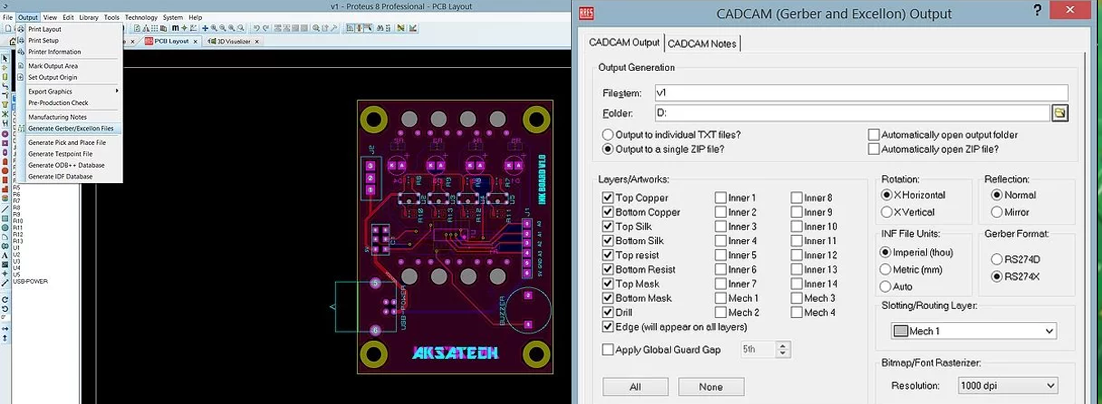
In this article, PCBP walks about how to produce a PCB that has been designed in the Proteus PCB design program and ordered from the pcbway.com site in China. The reason why he prefer Tile in this regard, is the cost of the service. It often costs $2~ $5 to make 2-layers PCB and that's awesome. In this post we will refer to the following topics in general just as PCBP did in his post.
- Get quick quotes from pcbway.com
- Paths and Vias
- Production of gerber file in Proteus
- Gerber file uploaded to pcbway.com and approval process
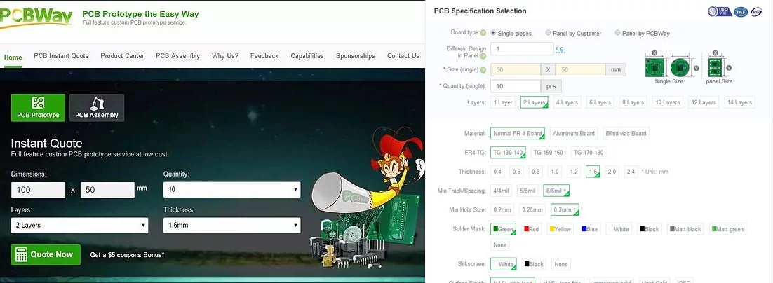
When you open the site you will see an interface like the one above. There are a few variables that you need to log in on this interface.
- PCB dimensions (mm) - Quantity to be produced - Number of layers in the card (Layers) - Thickness of PCBs Once you have entered all this information, you need to press the "Quote Now" button. After pressing this button, you will meet the following screenshot and will ask for some more detailed information about your PCB. Let's examine these options in detail.
-PCB Variety: In this section, selection of plate raw materials to be used in PCB production is made.
- Normal FR-4 Board: The most used raw material in the market is FR-4. It is produced from woven glass wool and epoxy components. Comfort comes to the forefront with its flexibility and lightness.
- Aluminum Board: Especially preferred for Power LED applications. The high thermal conductivity plays an active role in cooling the LEDs.
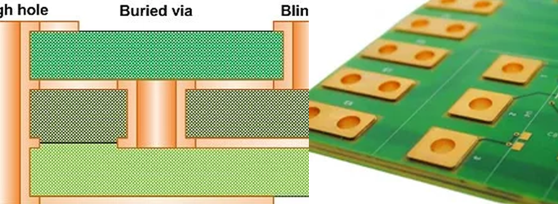
- Blind Vias Board: Via tiles must start on one surface and end on a layer before reaching the other surface. This type of application is a special board type. In the diagram below, the Blind Via difference clearly appears.
- HDI Board: HDI Board is a technology that makes it possible to produce PCBs of designs with complicated and compact structures like Telephone, Computer and Television.
- FR4-TG: This area defines the maximum temperature at which the PCB that we produce will be able to withstand. The higher the TG (Glass Transition Temperature) value, the less likely your PCB will be deformed in hot environments. Particularly in Power LED and Power Board applications, high thermal resistance PCB should be preferred.
Thickness: The area where the PCB thickness is selected. You can select a value for the purpose of your application. In general the selected value is 1.6mm.
Min Track / Spacing: You need to select the minimum distance between the tracks and the minimum distance between the tracks when you design the PCB. If you define your program rule during PCB drawing, you will be warned if the program goes out of the specified limits. Thus you are protected from unanticipated cost increases. Because as the distance decreases, production becomes difficult and therefore the price is increasing.
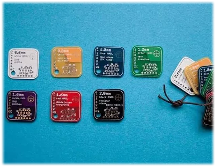
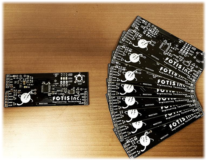
Solder Mask: You need to specify in this option which color will be coated on the PCB. Sample PCBs in different colors are given in the following photograph.
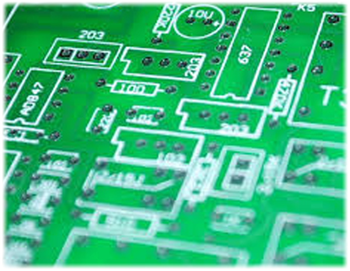
Silk Screen: The area where the fonts and shapes on the PCB are indicated. Choose the color you think is the most compatible to your chosen Solder Mask coloring.
Surface Finish: This option is used to select what the footprints of the components should be on the PCB.
- HALS (Hot Air Level Soldering ) with Lead: Includes pre-soldered connections. One of the cheapest and most preferred surface finishing techniques. It is more likely to oxidize.
- HALS (Hot Air Level Soldering ) with Lead Free: No pre-soldering. It is one of the cheapest and most preferred surface finishing techniques. It is highly likely to be oxidized.
- Immersion Gold: Produced on Nickel with gold plating technique. A surface termination technique that has been widely used in recent years for RoHs compatibility. It is quite expensive compared to other techniques.
- Gold - Hard Gold: Produced on Nickel with gold plating technique. It is more durable than Immersion Gold. It allows to be assembled and disassembled again and again. A surface termination technique that has been widely used in recent years for RoHs compatibility. It is quite expensive compared to other techniques.
- OSP (Organic Solderability Preservative): It is a coating method made with organic preservatives. It is a good preservative against oxidation.
- Finished Copper: This option determines the thickness of copper paths. The larger the copper density of the roads, the greater the path and the thicker it will be. For low-current signal paths, this thickness may not be sufficient for high-current supply cards and similar cards, while the 1 oz CU option is appropriate. You can visit the following web address to convert from oz to miles and other units of measure.
The photograph shows the paths with different copper thicknesses.
Via Process: 2 or more layered PCBs are available for covering vias that provide interlayer switching. The features of these options are listed below. - Tenting Vias: Via holes are completely covered with Solder mask. Closing the holes is an advantage in terms of corrosion prevention.
- Plugged Vias: Via holes are completely covered with Solder mask and filled in. Closing the holes is an advantage in terms of corrosion prevention.
- Vias not Covered: When this option is selected, the via holes will not be covered. The holes are high in risk of corrosion. But it is advantageous to take measurements from uncoated holes and to do similar work.
After selecting all options in the most appropriate and economical way, we press the "Quote Now" button again. After this process, the price window appears. We are making cargo company and country selection in this window. When choosing a cargo, you need to be aware of the "HK Post" option. When you choose this option, your products reach your hand within about 3-4 weeks, but at a rate of 5% chance of being attached to the customs. If you choose DHL, your product is 99% likely to be placed on customs. If you have to deal with customs costs and do not want to spend extra you need to stay away from DHL. As you can see, the 5cmx5cm size of 10 PCBs will cost $ 19. It costs about $2 per PCB. If you increase the number of PCBs by 2, the price you pay per PCB will decrease because the price will not double. Pretty cheap, is not it? !!! When you press the Add to Basket button, your order is added to the shopping cart.
