Earrings have been a hackers’ target for electronic attachment for quite a while, but combining the needed components into a package small enough to wear in that finicky location is quite a challenge. If [Sawaiz Syed]’s Art Deco Earrings are anything to go by, ear computers have a bright future ahead of them!
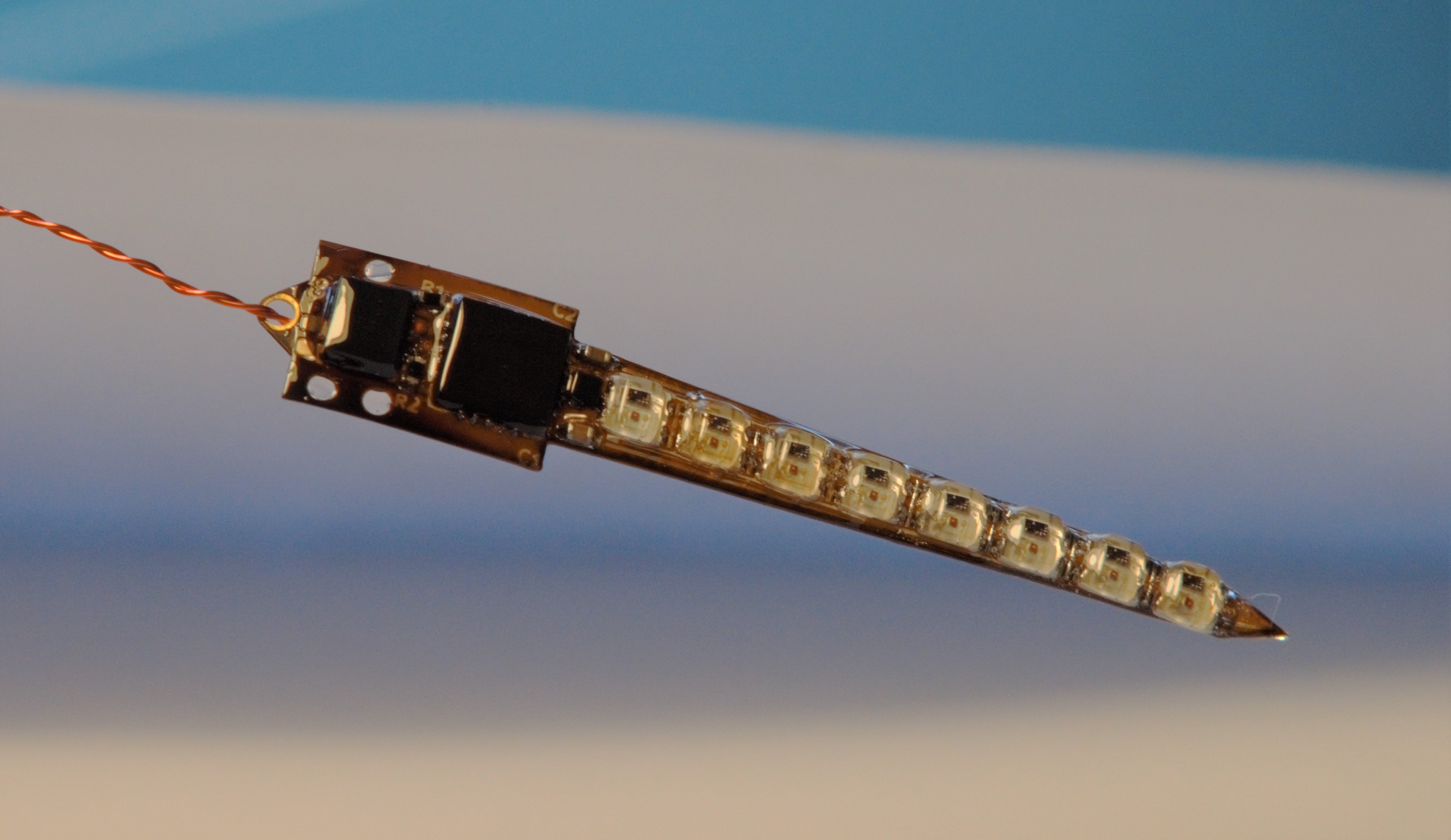
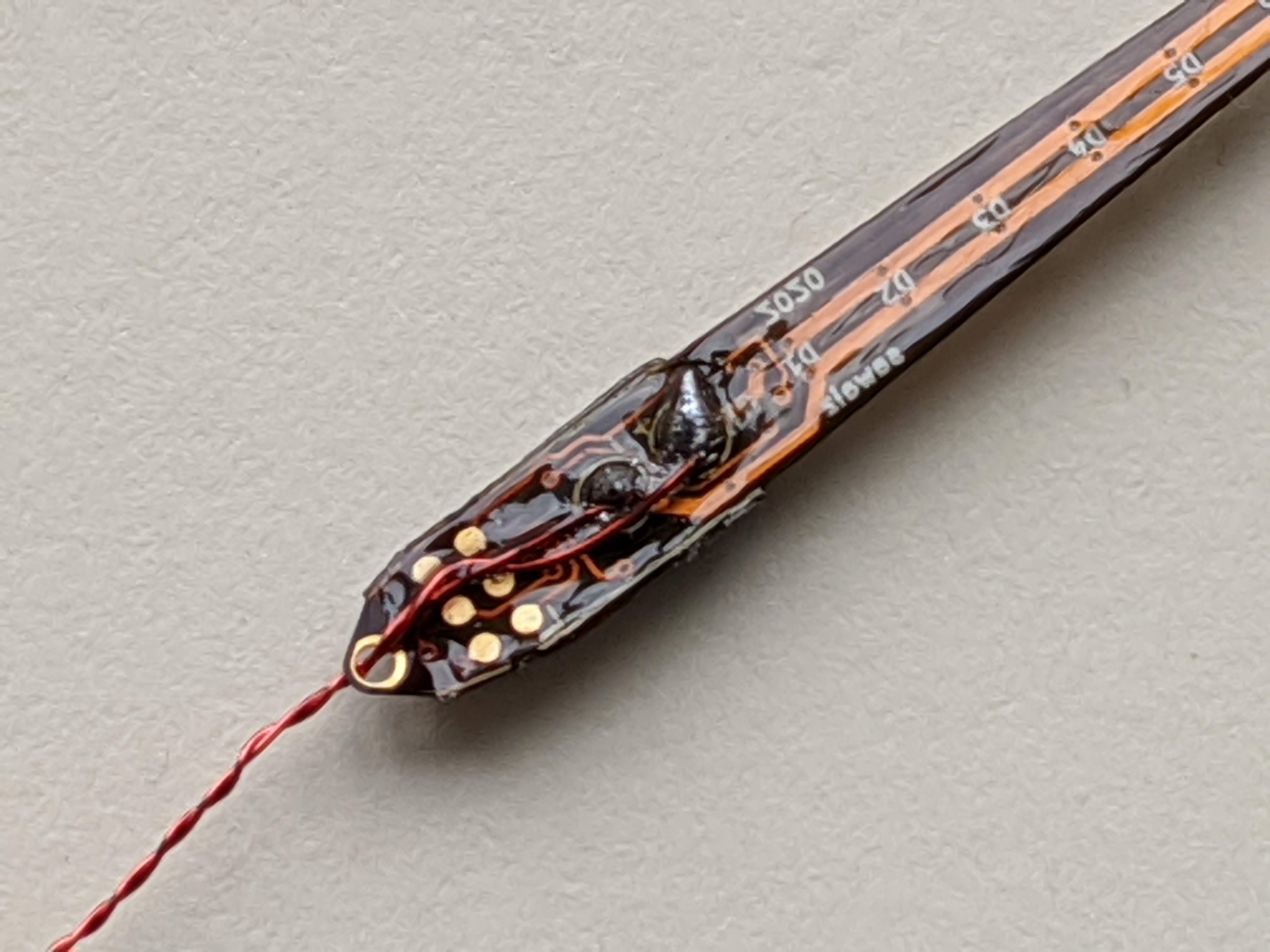
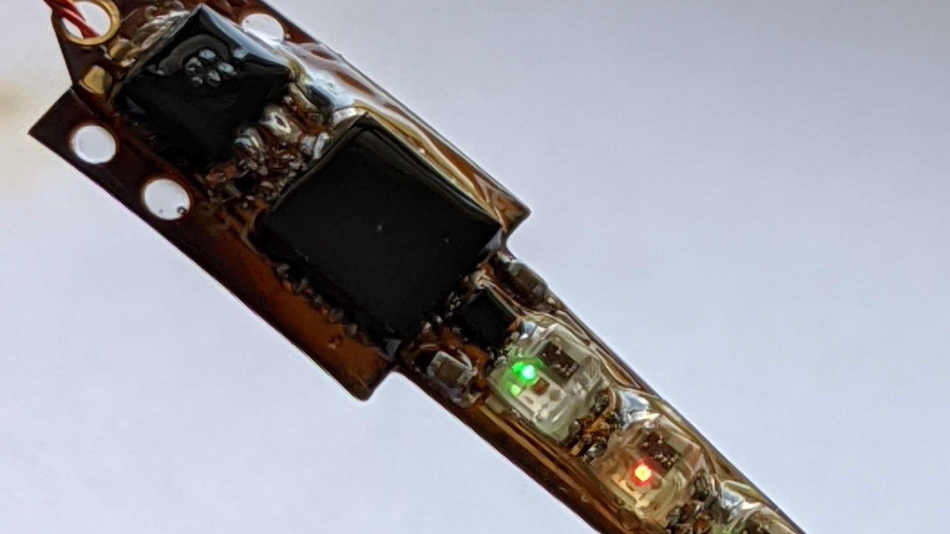
This is a project unusually well described by its name. It is in fact an earring, with art deco styling. But that sells it way too short. This sliver of a flex circuit board is double sided to host an ATtiny, accelerometer, LDO, and eight 2020 formfactor controller-integrated LEDs. Of course it’s motion sensitive, reacting to the wearer’s movement via LED pattern. [Sawaiz] makes reference to wearing it while dancing, and we can’t help but imagine an entire ballroom all aglow with tiny points of LED light.
The Art Deco Earrings are also set apart by the thoroughness of their documentation (have we mentioned how much we love detailed documentation?). [Sawaiz] not only drops the source in your lap, but the README in the Github repo linked at the top walks the reader through each component of the design in detail. Plus the PCBA render is so complete it includes a model of the wire loop to fit through the wearer’s ear; how cool is that? The single piece that’s still in progress is the battery. The earring itself hosts an LDO, so all that is required is stashing a battery somewhere discrete, perhaps in the user’s hair? We’re looking forward to seeing what [Sawaiz] works out.
For the full effect, check out the gif of an assembled unit in action after the break.
Power Supply
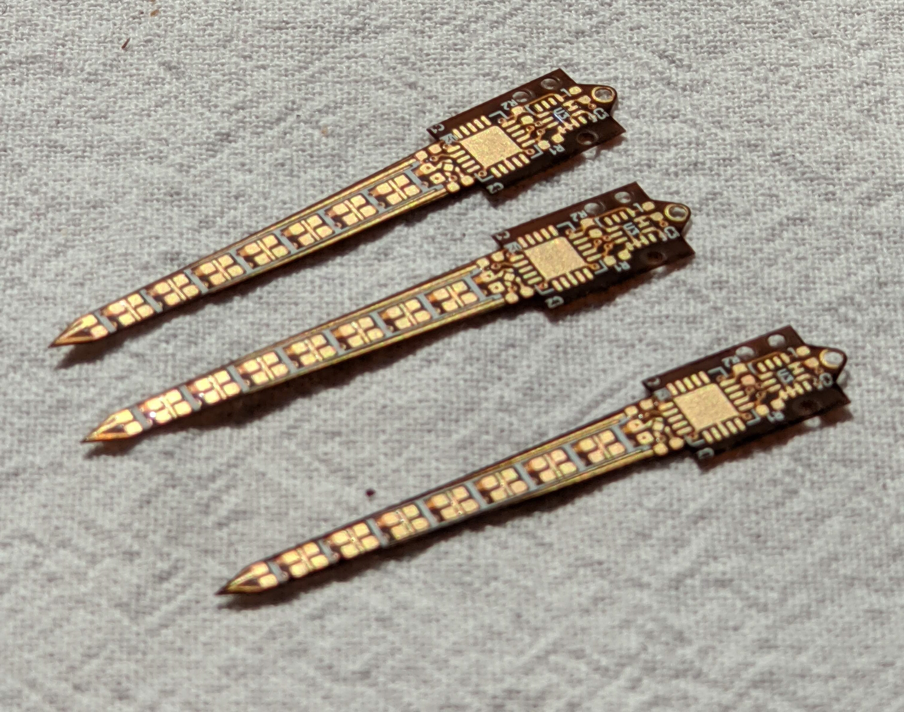
Microchip's MIC5365 and battery pads are the main power components. The 3.3V LDO linear regulator provides power to the microcontroller and IMU. There is no UVLO so it is recommended your battery has one. With voltage below 3.3V the output voltage corresponds to the input with the ~60mA drop, the board should continue working until 2.7V where the blue diode will cut out and the microcontroller falls out of it's speed grade and may not be able to maintain its clock speed. The two battery pads on the back are marked with plus and minus symbols and can have enameled wires soldered to them to provide power to the board.
Assembly is all surface mount with components on one side of the board to make PNP assembly easy. The layout layer duplicated below lists components by their reference designators and values. Solder paste can be applied with 25ga+ syringe, or with a stencil of the top paste layer. The components can then be placed, taking note of those that are polarity dependent, being U1-U3 and D1-D8 as marked in the assembly layer. A standard reflow profile, a hotplate, or a hot air rework station should work equally well. Inspect the side joints of the microcontroller as they will experience a lot of stress when trimming the board. The board is a two-layer polyimide flex with 6/6mil spacing, plated through vias. These are generally the defaults boards so they can be made by most fabrication houses provided flex is an available option.
If you also want PCBs, you might want to check the sponsor of the post, OURPCB and get a quote for your PCB design. Have a nice day!