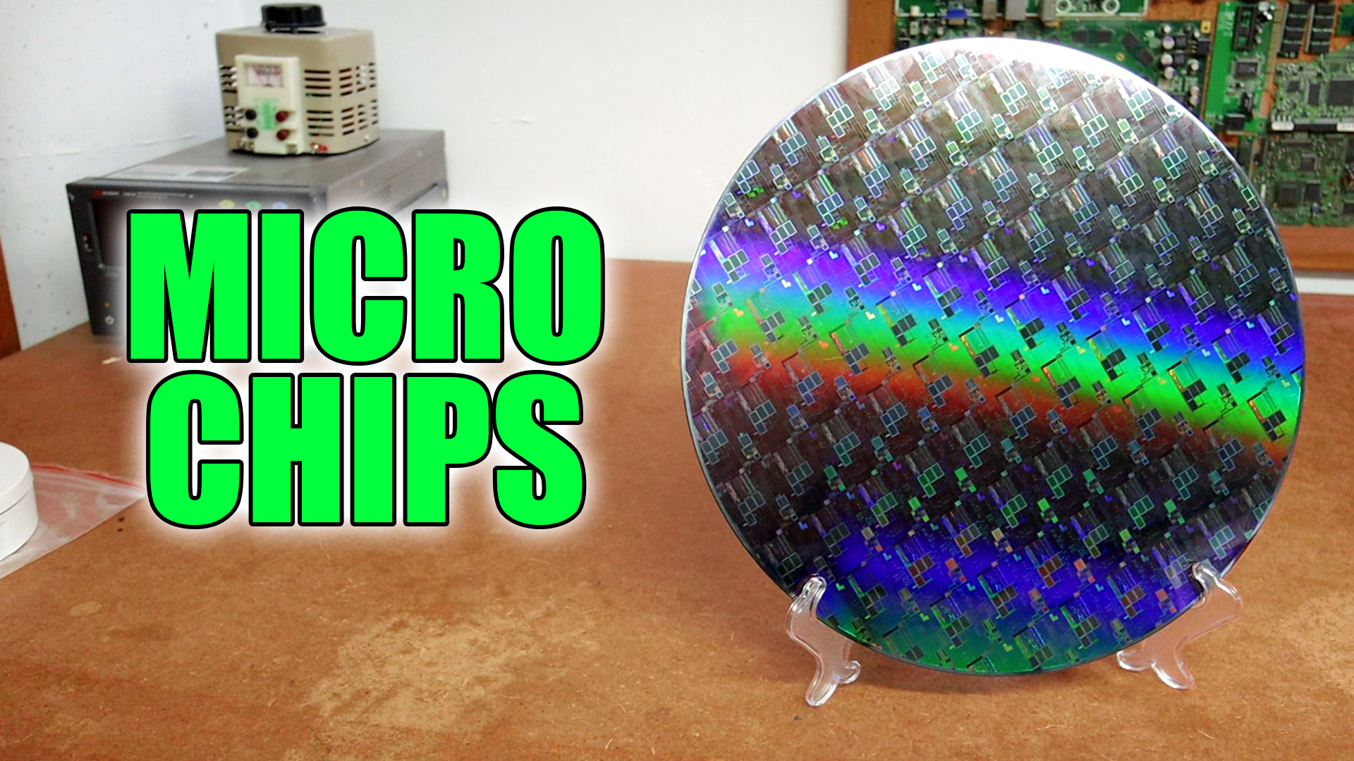
What’s up my friends, welcome back. I’ve bought this wafer to use as a reference for my video. I don’t even know from what microchip is it. It could be a memory, maybe a microcontroller or some sort of driver. Who knows. But as you can see, we have some sort of repeating pattern. That’s because microchips are not made 1 by 1. To speed up the process, reduce costs and use the entire area at once, microchips are made on a silicon wafer like this one or it could be even bigger. Then the wafer is cut to size and each microchip would go to its enclosure. For example I also bought these other chips that have the enclosure open so we could see inside it. This time we have only 1 microchip instead of an entire wafer. In order to protect the chip and also add external connectors, the foundry closes the chip inside this black epoxy material and also adds metal pins.

So, let’s start from the beginning. It all starts with one of the most abundant materials on earth. Sand. Or to be more specific, silica, or silicon. Microchips are made of silicon but in nature, usually, sand has silicon together with oxygen and we need pure silicon. For that they merge the silica sand with carbon and heat it up to extreme temperatures to remove the oxygen. after complex chemical and fiscal processes, we achieve pure silicon. When melted, they submerge a rod in and out just as a candle process. Each time the rod is submerged in the melted silicon, it gets bigger and bigger and that is how they create a pure crystalline silicon ingot called the boule. Once we have the boule is time to create the wafers so using special saws they cut the boule into very fine wafers of clean pure silicon. Now we have a brand new wafer with nothing on it. Is time for part two which is creating the transistors.
For that we start with the design of the chip. Microchips designing software are very expensive. For example, during my university time I had the chance to use Cadence software. You start with a circuit of transistors, and then you pass to the layout representing the different layers of the chip of those transistors. As an example let’s say we make just a simple NPN transistor. The layout would be something like this representing the N, the P and N area, the gate metal connection and so on.
For the next step, the wafer is introduced inside a reactor chamber and a thin layer of oxide is placed on top. This is non conductive for now. Then, for the next step, the wafer is filled with a photosensible solution that hardens under light. Using the layout designed before, the foundry creates a mask. That mask is placed in front of, usually, UV light, so it creates the pattern of the layout. This mask is very big compared with the nanometric size of the transistors. So usually, a set of mirrors and lenses are used to focus and reduce the mask light to the exact nanometric size. Now the photosensible solution hardens with the exactly shape of the layout.
The wafer is submerged into a cleaning solution to remove the solution that is not solid. Just like that we create the mask over the wafer. Then the wafer is etched using a chemical etching or a plasma process. So, the next step is to add other chemicals or a plasma chamber to remove the oxide that is exposed. Like that we create channels in the bulk oxide on top of the silicone. Then a deposition process is made inside a reaction chamber. The wafer is introduced inside a reactor and a small layer of a doped silicon, poly silicon, metals and so on, is applied. Let’s say we apply a N type doping. After that the mask is removed and we are left with this.