

1. What kinds of MOSFET breakdown are there?
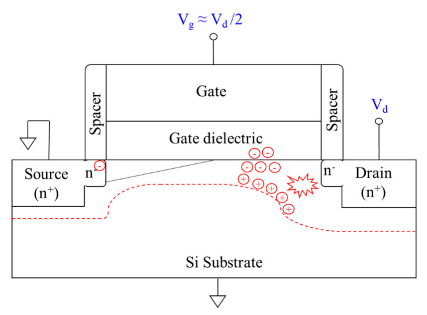
Let's talk about the test setup. The source and gate substrates are all grounded once the drain voltage has been scanned and the current at the drain terminal has exceeded 1 uA., according to easybom. In terms of device structure, the three leakage channels are drain to source, drain to bulk, and drain to gate.
1. Punch-through breakdown for drain to source
When the reverse bias voltage is applied to Drain, the depletion zone of the Drain/Bulk PN junction expands, which causes this. When the depletion region hits the source and creates a passage between the source and the drain without opening, it is known as punch-through ( punch through).
So, how do you avoid punch-through? This has to do with the reverse bias property of the diode. The voltage and doping concentration on both sides have a direct relationship with the depletion region's width. As the concentration rises, the depletion region can be prevented more broadly. Keep in mind that it must also play the same kind of specis (Punch Through).
Naturally, the BV that really came into contact with WAT ran, and it was confirmed that it wasn't there on the Source side any longer. It might also depend on whether the problem is with PolyCD, Spacer, or LDD IMP's width.
Can you completely rule it out? Whether NMOS and PMOS are both active determines the situation. POLY CD can be verified via poly-related WAT.
Several characteristics are linked to punch-through breakdown:
On the other hand, a high depletion layer spread makes the source-substrate junction susceptible to the DIBL effect, which results in a progressive increase in current at the junction.
(2) The soft breakdown point of punch-through breakdown is where the source and drain depletion layers converge. The electric field in the depletion layer at this point causes the carriers at the source end to be injected into it, where they are then driven to the drain end.
As a result, in contrast to the current during the avalanche collapse, the current during the punch-through breakdown has a strong rising point. The avalanche current dominates the breakdown current during the reverse breakdown of the PN junction.
(3) Destructive failure is not necessarily the outcome of punch-through failure. Because the punch-through breakdown field strength is not greater than the avalanche breakdown field intensity, a large number of electron-hole pairs will not develop.
(4)Punch-through breakdown occurs largely in the channel body; the channel surface is not susceptible to punch-through. This is due to the channel injection, which raises surface concentration above concentration. As a result, punch-through injection is typically avoided by the NMOS tube.
(5) Punch-through breakdown happens in the middle of the channel because the concentration is often higher there than it is in the middle of the beak.
(6) The length of the polycrystalline gate has an impact on the punch-through breakdown. As the gate length increases, the breakdown increases. It also affects avalanche breakdown strictly speaking, but the impact isn't as great.
2. The disintegration of a drain-bulk avalanche
This is an avalanche breakdown of the PN junction. The fundamental reason for this is that under the reverse bias voltage of the drain, the depletion zone of the PN junction is enlarged, and the reverse bias electric field is applied to the reverse bias of the PN junction, driving the electrons to accelerate and impact the lattice. When the electrons continue to collide, more electron-hole pairs are produced, which causes the avalanche to grow and eventually break down. Because of this breakdown's nearly vertical spike in current, burning is made incredibly simple. (Not to be confused with the punch-through breakdown of the source-drain system.)
So, how can this intersection be made better? Due to the characteristics of the PN junction itself, it is necessary to reduce the electric field in the depletion area to prevent collisions from creating electron-hole pairs. The breadth of the depletion region can only be increased because it is difficult to lower the voltage, necessitating a change in the doping profile. This explains why the breakdown voltage of the abrupt junction is lower than that of the graded junction.
Of course, in addition to the doping profile, there is also the doping concentration. Because the depletion region gets smaller as concentration rises, the electric field intensity increases with decreasing breakdown voltage. Another rule is that because the depletion region is broader, the concentration on the lower concentration side has a bigger effect on the breakdown voltage.
The equation is BV=K*(1/Na+1/Nb). Also, the calculation demonstrates that if the concentrations of Na and Nb are ten times different, practically one of them can be disregarded.
If the BV drops during the actual process and it is determined that the junction is to blame, check your Source/Drain implant.
3. Drain-Gate failure
This is mostly owing to the Overlap between the Drain and the Gate, which causes the gate oxide layer to collapse. This resembles the GOX breakdown quite a little. Naturally, it's more akin to a GOX breakdown of the Poly finger, thus he'll need to take additional care to avoid sidewall damage and poly profile damage. Of course, GIDL, which will result in leakage and lower BV, is another problem with this Approach.
As can be seen above, the MOSFET is broken down into three channels. The BV cases are often the first two.
In the off-state, when the Gate is at 0V, the breakdown described above occurs. But, when the Gate is turned on, the voltage sent to the Drain may be too high, resulting in breakdown. We term it an on-state breakdown.
It is almost always NMOS and most usually occurs when the gate voltage is low or when the tube has just been turned on. We typically WAT BVON as a result.
2
How do you handle the critical circumstance where a mos tube is being heated by a little current?
When developing power supply or driving circuits, MOS tubes cannot be avoided. MOS tubes are available in a range of forms, sizes, and applications. Of course, a power supply's or drive's switching capability is utilized.
Whether the MOS tube is N-type or P-type, the operating principle is substantially the same. The MOS tube's output terminal's drain current is controlled by the voltage applied to the gate of the input terminal.
The MOS tube is a voltage-controlled device. The charge storage effect caused by the base current when the triode is switched is avoided, and the device's characteristics are controlled by the voltage applied to the gate. As a result, in switching applications, the MOS tube's switching speed ought to be faster than that of triodes.
MOS tubes' PDF properties are frequently studied. Manufacturers of MOS tubes utilize the RDS(ON) parameter to specify the on-resistance. The most important device feature for switching applications is RDS(ON).
Although RDS(ON) is a relatively static feature for an acceptable gate drive, it is described in the data sheet in relation to the gate (or drive) voltage, VGS, and the current flowing through the switch. The always-on MOS tube heats very quickly. Furthermore, gradually increasing junction temperature will result in a rise in RDS (ON).
The MOS tube data sheet contains information about the thermal impedance parameter, which is the MOS tube package's capacity to dissipate heat from the semiconductor junction. The simplest definition of RJC is the heat resistance between the junction and the casing.
1. The mos tube is heated by a modest current for the following reason:
Making the MOS tube operate in a linear working state as opposed to a switching state, which is one of the causes of the MOS tube's heat, is an issue with the circuit design.
An N-MOS switch's G-level voltage is a few volts higher than the power supply's full-on voltage, but a P-MOS switch's G-level value is the opposite. The equivalent DC impedance is relatively high, the voltage drop increases, so U*I increases, resulting in heat generation. The voltage drop increases, so U*I increases, resulting in heat generation. It is not fully turned on, and the voltage drop is too big, resulting in power consumption. The most hated mistake in circuit design is this one.
2) There is an excessive frequency: The primary cause is that the volume is occasionally sought excessively, which increases frequency and increases loss on the MOS tube, resulting in increased heat generation.
3) The heat dissipation design is inadequate; the MOS tube's nominal current value necessitates good heat dissipation, yet the current is too high. Because of this, if the ID is lower than the maximum current, it could produce a lot of heat and call for the usage of additional heat sinks.
4) The choice of the MOS tube is erroneous; the power estimation is flawed, and the internal resistance of the MOS tube is not fully taken into account, increasing the switch impedance.
2. How to effectively deal with the serious heating of mos tubes using low current
(1)0 Design the MOS tube's heat dissipation well, and include enough auxiliary heat sinks.
(2)Affix a heatsink.
3. Why is it possible for the MOS tube to stop the power supply from being flipped?
Reversing the power source is an inevitable circumstance, but it will harm the circuit. We must incorporate a protective circuit into the circuit in order to achieve the objective of remaining intact even if the power source is switched around.
Connecting a diode to the positive pole of the power source can usually fix the problem. Unfortunately, due to the diode's voltage drop, the circuit will incur severe losses, especially in the case of battery power. V, greatly decreasing battery life.
The low voltage loss while utilizing MOS tubes for anti-reverse connections is a benefit. The current MOS tube can have an internal resistance of several milliohms if the internal resistance is 6.5 milliohms, the current passing through is 1A (which is already a huge current), and the voltage drop is just 6.5 millivolts.
As MOS tubes become more affordable, people have progressively started using them to prevent reverse power connections.
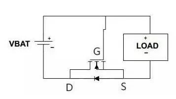
An NMOS tube to stop a circuit using a reverse power supply:
When connected properly: Shortly after the power is turned on, the MOS tube's parasitic diode activates, turning the potential of S to about 0.6V and the potential of the G pole to VBAT. The MOS tube's DS will switch on because VBAT-0.6V is higher than UGS's threshold voltage. Because to the low internal resistance, the parasitic diode is short-circuited, and voltage loss is almost nonexistent. The MOS tube won't switch on when the power is reversed, UGS=0, and the loop with the load will be broken, guaranteeing the circuit's safety.
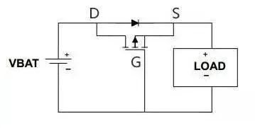
A PMOS tube to stop a circuit with a reverse power supply:
When properly connected: The power supply and load create a loop, the parasitic diode of the MOS tube turns on shortly after the power is turned on, the S pole potential is VBAT-0.6V, the G pole potential is 0V, the PMOS tube turns on, and the current flowing from D to S short-circuits the diode.
When the power is switched around, the G pole is elevated and the PMOS tube is not activated. Ensure the safety of the circuit.
Skills for connections: Tube NMOS The PMOS tube's negative pole is wired to DS. DS is connected to the positive pole, and the parasitic diode is facing the right connection current direction.
Has your DS flow been "reversed"? Those with keen eyes will observe that the anti-reverse circuit's current direction of DS is the exact opposite of the current direction we typically use.
Why would you reverse it? When the power is first turned on, the UGS can satisfy the threshold criterion using the parasitic diode's conduction effect.
Why is that possible? NPN and PNP can only move in one direction, C to E and E to C, respectively, if the device is a triode. One of the differences between the triode and the MOS tube is that the D and S of the MOS tube are interchangeable.
4. Measurement of power loss in 4 MOS tubes
Yet, many engineers still use perceptual cognition and manual computation to assess switching loss, and the switching loss of PFC MOSFET can only be determined by word-of-mouth experience. The switching loss test of MOSFET/IGBT is a crucial link in power supply troubleshooting. How can the evaluation be quantified after repeated exploration?
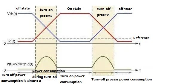
1. A schematic and observed power loss diagram
The schematic diagram of the switching tube's power loss is illustrated in Figure 1 in general. The majority of the energy loss is indicated by the "on process" and "off process," with the "on state" representing only a small percentage of it. The loss is so insignificant that it is easy to ignore.
2. A comparison of MOSFET and PFC MOSFET performance
With conventional MOS tubes, the voltage and current waveforms of various cycles are essentially identical, making it possible to arbitrarily determine the overall power loss for one cycle.
With PFC MOS tubes, different cycles produce distinct voltage and current waveforms, hence accurate power loss estimation necessitates waveform capture for a lengthy period of time (often greater than 10ms) and a higher sampling rate. The required storage depth is larger than 10M, and the power loss estimate must take into account all raw data (which cannot be sampled). The measured snapshot is displayed in Figure 3.
I now understand how to address the issue of low current heating of MOS tubes.


Figure 5